https://publons.com/researcher/1640912/yumeng-shi/
https://orcid.org/0000-0002-9623-3778
Research Introduction
▲citation times
My research career specializes in the synthesis of various two-dimensional (2d) materials including semiconducting transition metal dichalcogenides (TMDCs) monolayers (MoS2, MoSe2, WS2, WSe2), insolating h-BN and semi-metallic graphene using chemical vapor deposition (CVD). With these materials, we further develop their various applications in the fields of field effect transistors, sensors, energy storage devices and catalysis.

The synthesis of graphene layers and 3D graphene networks
I started to build up my first homemade CVD systems since 2009 in the department of Electrical Engineering and Computer Science at Massachusetts Institute of Technology (MIT). We synthesize high quality graphene layers by CVD method on nickel thin films, 3d metal foams and copper foils. The graphene layers were used in various applications, including biosensors, solar cells, energy storage devices and photodetectors. (ACS Nano, 4, 2689, (2010), ▲ 271; Advanced Materials, 22, 1649, (2010), ▲ 272; Small, 9, 3433, (2013), ▲ 267) We are the very first group to demonstrate 3D graphene based electrodes produced by CVD method for supercapacitor applications, which has later become one of the most important graphene form for energy storage due to its high electrical conductance and large surface area. (Small, 7, 3163, (2011), ▲ 511;)

CVD of monolayer and few layer h-BN
Based on the studies on graphene, we soon realized the graphene layers are very sensitive to environmental charges and surface absorbance. (Physical Review Letters, 102, 135501, (2009), ▲ 155, PHYSICAL REVIEW B, 79, 115402, (2009), ▲129) The research society on graphene study has widely accepted that to obtain the intrinsic high mobility of graphene, the quality of substrate-supporting materials are critical. Hexagonal boron nitride (hBN) is a pivotal component in two-dimensional van der Waals heterostructures as a high-quality insulating material due to its large energy gap and chemical-mechanical stability. In 2010, we have successfully synthesized few-layer hexagonal boron nitride thin film by chemical vapor deposition (Nano Lett. 2010, 10, 4134; ▲ 410). We have achieved high quality and large-area h-BN, which was thought to be very challenging before. (United States Patent US8592291). This work pave the way for high performance graphene electronics. The synthesis of h-BN also lead to many other subsequent works including the application of h-BN as dielectric materials and direct growth h-BN/graphene heterostructures. (Nano Lett. 12, 161, (2012), ▲ 342; ACS Nano, 6, 8583, (2012), ▲ 152) So far, synthetic h-BN has been widely used in the society to build many artificial 2d crystals exhibiting many novel properties.

CVD synthesis of MoS2, and MoS2/Graphene Heterostrucutres
During 2011-2012, we began to work on the synthesis of semiconducting molybdenum disulfide, a 2d semiconducting material exhibiting a better photoresponsivity as compared with the graphene-based devices (ACS Nano, 6, 74, (2012), ▲ 1159). We are the first to produce monolayer MoS2/Graphene heterostrucutre using (NH4)2MoS4 as growth precursor and revealed the van der Waals epitaxial growth mechanism (Nano Lett. 12, 2748, (2012),▲ 428). Meanwhile, by the thermolysis of the same precursor, thin layer of MoS2 was further successfully synthesized on dielectric materials showing excellent semiconducting behaviors, (Nano Lett. 12, 1538; (2012), ▲780). The works on isolation and synthesis of MoS2 monolayers stimulated the research area of growth of TMDC layers. The first integrated device based on MoS2 has also been demonstrated with our CVD materials (Nano Lett. 12, 4674 (2012); ▲665).

Lateral stitched WSe2-MoS2 monolayer with atomically sharp interface
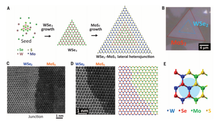
Since 2014, I became a research scientist in King Abdullah University of Science & Technology (KAUST) to study advanced transition metal dichalcogenide materials and create perceptive projects. After joining KAUST, we have further shown the direct growth of atomically sharp p-n junction between WSe2 and MoS2. (Science, 349, 524 (2015); ▲156). This demonstrates the state-of-the-art growth in this field. The heterostructural interface presents a nice p-n junction, which is a key component for monolayer electronics. Most critical components in modern electronics/optoelectronics can be redesigned and produced based on this new class of 2D materials, where the great ability to tune the band gap, band offset, carrier density, carrier polarity and switching characteristics provide unparalleled control over device properties and possibly new physical phenomena. With close collaboration works with KAUST community, we developed a photoresist-free method of monolayer TMDC patterning. (ACS Nano, 10, 10516, (2016) ▲3) The patterned monolayer TMDCs can be used to form lateral TMDC heterostructures directly on the sapphire substrate. Devices fabricated on the synthesized TMDC heterostructure show excellent stability and obvious rectification behaviors in the I−V measurements. The photoresist-free lithography and epitaxial edge growth strategy developed here offer opportunities to construct various two-dimensional lateral devices. The new electronics based on 2DL materials is hence called “monolayer electronics”. Our research opens the path leading to future monolayer electronics.

Defects engineering of 2d monolayers and exciton emission enhancement
TMDC monolayers grown by CVD may incorporate structural defects, (Nano Lett, (2013, 13, 2615, ▲427)) these defects can significantly trap free charge carriers and localize excitons, leading to the smearing of free band-to-band exciton emission. In 2016, we have developed a simple hydrohalic acid treatment (such as HBr) to suppress the trap-state emission and promote the neutral exciton and trion emission in defective MoSe2 monolayers. (ACS Nano, (2016), 10, 1454, ▲24) With the initial success, we are currently developing a more convenient method for the defects repairing of 2d crystals using inorganic salts. These results provide further insights of the control and tailoring the exciton emission from CVD-grown monolayer and push the quality of synthetic 2d monolayer to a new level.
With the knowledge from the CVD growth, we have published several review papers and 2 book chapters to teach the society and advertise the materials (Chemical Reviews, DOI: 10.1021/acs.chemrev.7b00212 (2017); Chemical Society Reviews, 44, 2744 (2015), ▲142; Nano Energy, 18, 293, (2015) ▲26; Materials Today, 19, 322, (2016), ▲20).
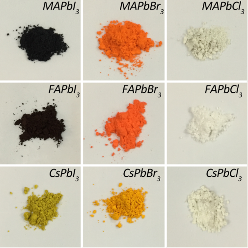
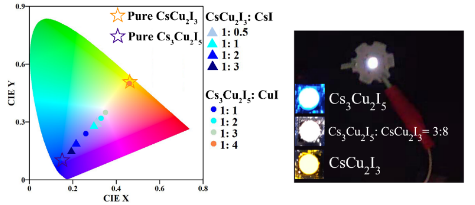
We further developed several novel synthetic approches for perovskite and perovskite related materials, and developed optoelectronic devices including photodetectors, ligth emitting diodes, light emitting transistors, and solar cells based on these materals.

J. Mater. Chem. A, 2019, 7, 540,https://doi.org/10.1039/C8TA08868C

Journal of Materials Chemistry C, 2020,8, 4895-49012020, https://doi.org/10.1039/D0TC00015A
We are more than happy to collaborate with friends worldwide to explore the applications of 2D and Perovskites nano materials for their applications in the fields of Solar Cells, Lasering, Transistors, Photodetectors, Light Emitting Diodes, Ion Batteries, Catalysis, and et al.
For further information please contact Prof. Yumeng Shi by email: yumeng.shi@szu.edu.cn
![]()