Two-dimensional nano optoelectronic laboratory Leader: Shi Yumeng
In this paper, we report a controllable CVD-grown monolayer MoS2 and layer-by-layer pyramidal-structured MoS2 crystals with an oxidized Mo foil precursor. The interlayer screening effects and charge conduction mechanisms in the pyramidal-structured MoS2 crystals are studied. Although the Fowler−Nordheim (FN) tunneling model is widely adopted to describe the vertical charge transport mechanism at the 2D semiconductor/bulk metal interface, we found that such a mechanism cannot satisfactorily explain the electrical measurement obtained from our CVD-grown MoS2 samples. Instead, our analysis reveals that Richardson−Schottky (RS) emission is the dominant transport mechanism when Vbias < 1 V. Our findings provide a fundamental understanding of the charge conduction mechanism in CVD-grown MoS2 crystals, which is crucial for development of MoS2 electronics and optoelectronics devices.

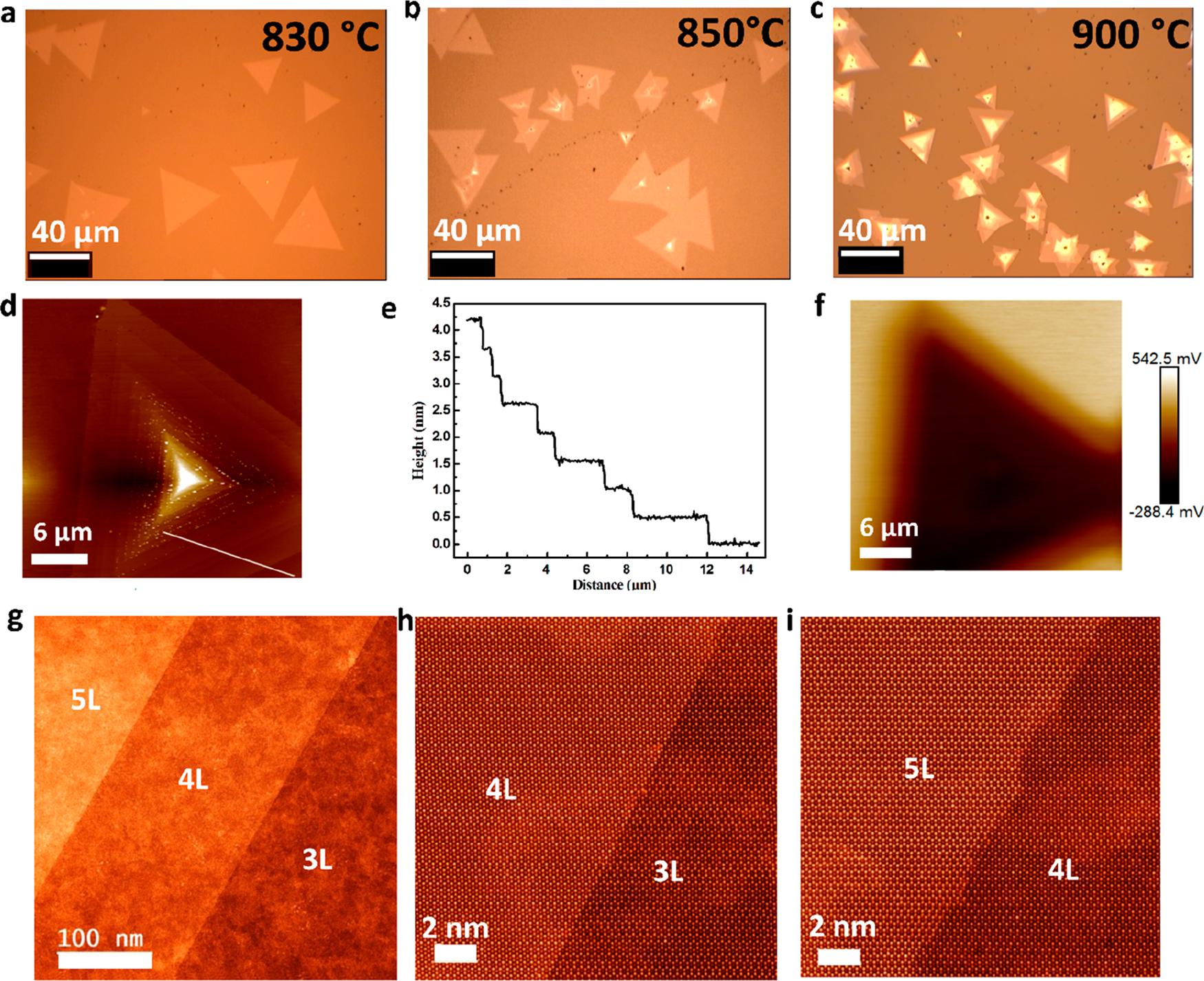
(a−c) Optical images of MoS2 crystals on sapphire. (d) Topography mapping image, (e) Topography profile along the line indicated in (d), and (f) SKPM surface potential of pyramidal-structured MoS2 crystals. (g−i) STEM-ADF images of pyramidal-structured MoS2 crystals.

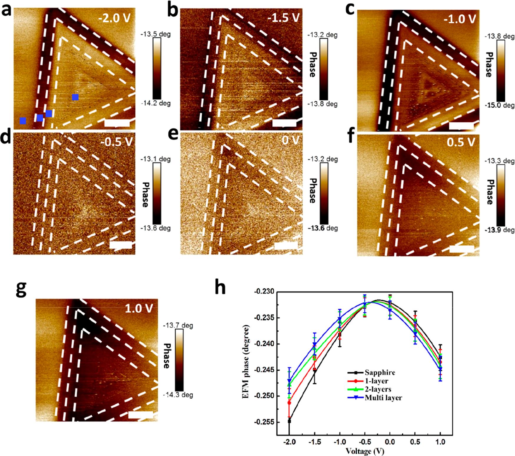
(a−g) EFM characterization of a pyramidal-structured MoS2 crystal. The scale bars in are 6 μm. (h) Curve of the EFM phase as a function of Vtip for the monolayer, bilayer MoS2, multilayer MoS2, and sapphire substrate.

Conclusions
In conclusion, we have developed a controllable CVD growth method to produce large-area monolayer and pyramidal-structured MoS2 crystals. Vertical charge injection can be achieved with a voltage less of than 1 V via the RS transport pathway due to the image potential-induced barrier lowering effects, thus revealing a potential route toward low-bias vertical charge injection in atomically thin TMDC without the need for a high-bias FE mechanism. Our work provides fundamental understanding on the vertical charge transport mechanism of the pyramidal-structured MoS2 crystals. These finding shall be beneficial for the development of 2D-material-based nanoelectronics
and optoelectronics applications.
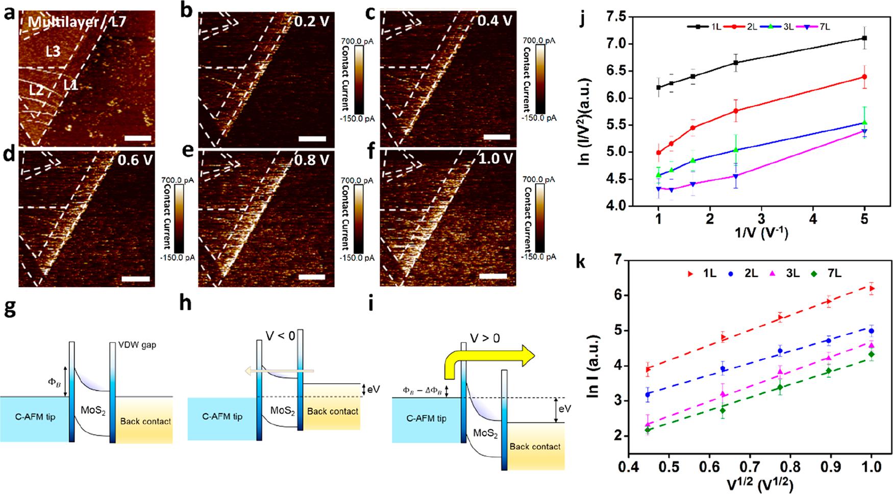
Layer dependence of charge transport in pyramidal-structured MoS2 crystals. (a) AFM image of pyramidal-structured MoS2 crystals. (b−f) Current image mappings of pyramidal-structured MoS2 crystals with applied voltages of 0.2, 0.4, 0.6, 0.8, and 1.0 V, respectively. Scale bar: 5 μm. (g−i) Schematic illustration of the band diagram of a thin layer MoS2−metal tip junction in equilibrium. (j) Fitting curves with mono-, 2-, 3-, and 7-layer MoS2 in the forward bias voltages. (k) Schottky emission model fitting curves for mono-, 2-, 3-, and 7-layer MoS2 in the forward bias voltages.