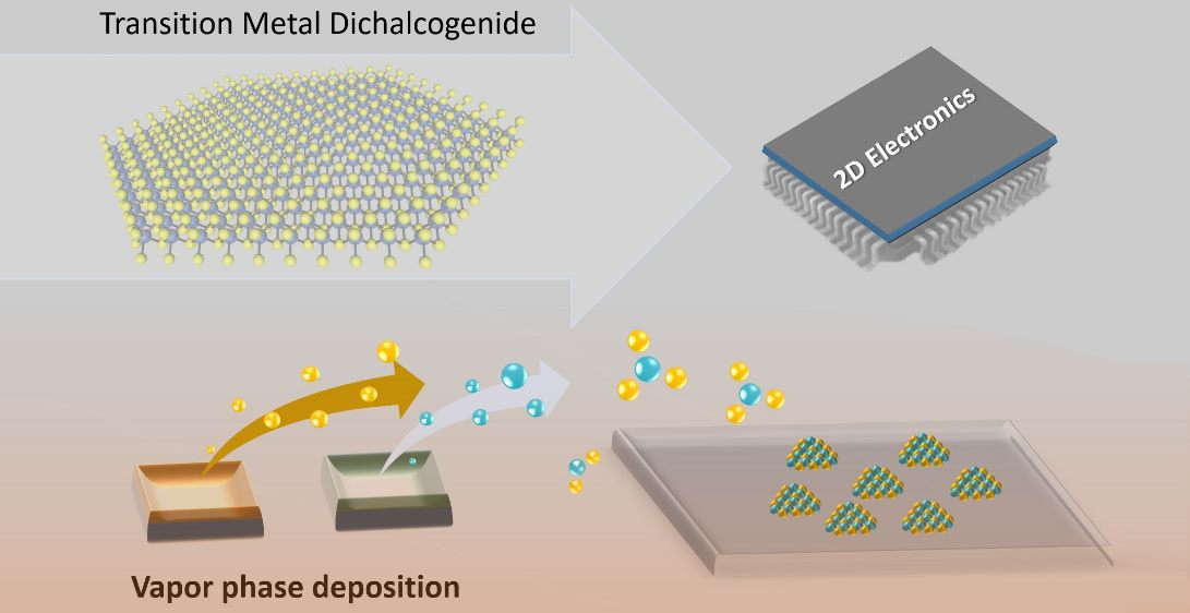
Toward the Growth of High Mobility 2D Transition Metal Dichalcogenide Semiconductors
Henan Li, Jing-Kai Huang, Yumeng Shi,* and Lain-Jong Li*
DOI: 10.1002/admi.201900220
Adv. Mater. Interfaces 2019, 1900220
The development of integrated circuits greatly relies on the continuous dimension downscaling in material size and thickness. However, the miniaturization of silicon-based transistors is facing fundamental limitations and the geometry scaling trend for silicon-based microelectronics is becoming plateaued. With the continuous scaling of the gate length, overlapping junctions may lead to short channel effects degrading the transistor performance. Two-dimensional (2D) monolayers, especially layered transition metal dichalcogenides (TMDCs) have emerged as a new class of materials, which offer several attractive features for electronic devices, including excellent thermal stability, flexibility, tunable bandgap, and high mobility. This review focuses on the key factors that determine the electrical performance of 2D TMDCs. From the device fabrication point of view, the interfacial properties between 2D TMDCs, electrode contacts, substrates, dielectric layers, and ambient environment dominate the device performances. Recent efforts on surface engineering for achieving high carrier mobility in TMDCs are reviewed. Fundamentally, the mobility of 2D materials is often hindered by charge scattering mechanism from the lattice defects or grain boundaries. The growth of high-quality TMDCs monolayers is essentially important for the large-scale fabrication of TMDCs-based integrated circuits. This paper further gives the outlook for future research directions, challenges, and possible development for 2D semiconducting electronics.

